
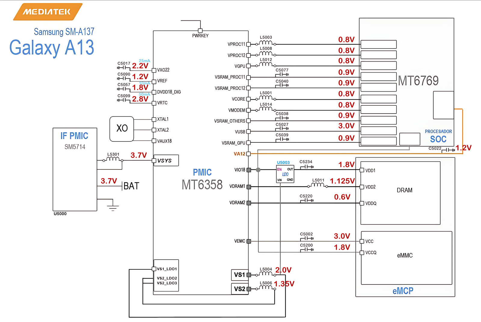
Voltage Distribution in Samsung Galaxy A13 (SM-A137) MT6358 PMIC
Introduction to the Power Management System
The Samsung Galaxy A13 (SM-A137) uses the MT6358 Power Management Integrated Circuit (PMIC) to manage the distribution of power across various internal components of the device. This chip is responsible for regulating the power from the battery and ensuring that each component receives the correct voltage for optimal operation. In this article, we will delve into how different voltage rails are handled, why they are necessary, and how they power the key sections of the phone.
Voltage Rails in the Galaxy A13
The MT6358 PMIC is responsible for converting and distributing power to several components inside the Galaxy A13. The power management IC regulates various voltage levels, ensuring each part of the system receives the appropriate voltage. The main voltage rails in the Galaxy A13 are:
- 3.7V (VSYS): The primary power source derived directly from the battery. It powers the PMIC and other key systems within the phone.
- 2.8V: This voltage is required for some sensors and low-power components.
- 2.0V: A power rail for certain peripheral components and sub-circuits in the device.
- 1.8V: Used for powering key components like the processor's power section and various peripherals.
- 1.2V: Provides power to the processor (SOC) and other core components requiring high-performance operation.
- 1.35V (VS2): This voltage is used for high-performance modules, such as advanced sensors or the power management system of some chips.
- 0.9V: A voltage used for specific sections of the processor (SOC) or GPU that require low voltage for stable operation.
- 0.8V: The low voltage used for some core parts of the device, ensuring efficient power consumption.
- 0.6V: Typically used by low-power devices or power-saving subsystems.
- 1.125V (VDram): This voltage rail provides power to the DRAM, enabling fast access to memory.
- 3.0V (eMMC): This voltage is used to power the eMMC storage for reading and writing data.
Understanding the Components and Power Pathways
As shown in the schematic, the PMIC plays a key role in regulating these voltages and distributing them to the appropriate sections. Here is an overview of the key components:
PMIC - MT6358
The MT6358 PMIC, located at the heart of the power system, is the main component responsible for ensuring that the correct voltage is delivered to the various systems within the phone. The PMIC takes input from the 3.7V battery and converts it into multiple regulated voltages for different subsystems.
Voltage Regulation Through LDOs and Buck Converters
The MT6358 uses a combination of Low Dropout Regulators (LDOs) and buck converters to regulate the input voltage. These components step down the voltage from the battery to the required levels for each component:
- 1.8V LDO (U5003): Used for powering the processor's core and other power-hungry components.
- 0.8V LDO (U5000): Ensures that the low-power sections of the processor, GPU, and other components receive enough power.
- 0.6V LDO: This LDO helps provide a very low voltage for highly efficient power management, especially for low-power components.
- 1.35V (VS2) Buck Converter: This regulator is used to deliver stable power to high-performance modules, ensuring that the voltage is consistently provided under heavy load.
- 1.125V (VDram) LDO: Powers the DRAM modules, enabling quick memory access.
- 3.0V for eMMC: Regulates the 3.0V voltage needed by the eMMC storage module for proper read/write operations.
Power Distribution Paths
The power from the 3.7V battery is routed through the PMIC, which directs the voltages to different components. Some key pathways are:
- Processor (SOC): The processor requires multiple voltage rails such as 1.8V, 2.0V, and 0.9V to handle various processing tasks and to maintain system stability during heavy tasks.
- DRAM: The DRAM requires a stable 1.125V supply to ensure proper data storage and retrieval at high speeds.
- eMMC Storage: The eMMC module uses 3.0V to manage read/write tasks for the device’s storage needs.
- GPU and RAM: The GPU, along with specific sections of the RAM, operates at 0.9V, ensuring smooth graphics rendering without overheating.
- Sensors and Other Modules: Various sensors and peripheral components receive specific voltages like 2.8V and 1.2V to ensure proper functionality.
Why These Voltages Are Important
Each voltage rail has a specific purpose within the phone. Here’s why these voltage levels are crucial:
- Processor Power: The processor requires multiple voltage levels (1.8V, 2.0V, and 0.9V) to handle various processing tasks. The power management ensures efficient use of resources without overheating the device.
- Memory and Storage: DRAM requires 1.125V for fast memory access, while eMMC storage requires 3.0V to read and write data effectively. A stable voltage is crucial for these components to function at peak performance.
- Graphics Processing: The GPU operates on 0.9V, ensuring that power consumption remains low while rendering graphics efficiently for a seamless user experience.
- Power Efficiency: Lower voltages like 0.6V are used for power-saving subsystems to ensure that energy is used efficiently, extending battery life.
Conclusion
The MT6358 PMIC is a critical component in the Galaxy A13, managing the distribution of power across the device. It ensures that each component receives the correct voltage required for optimal performance. By using a combination of LDOs and buck converters, it efficiently manages the power, improving battery life and performance. Understanding the role of the PMIC and voltage distribution in the device gives a deeper insight into how smartphones operate effectively and efficiently.