
Power Distribution in Samsung Galaxy A04 (SM-A045) using MT6357 PMIC & MT6765 SoC
The Samsung Galaxy A04 (model SM-A045) is powered by a MediaTek MT6765 (Helio P35) processor and uses the MediaTek MT6357 PMIC (Power Management IC) to manage the voltage regulation for various components.
🔌 Main Power Source
The primary voltage source is the battery (VBAT) which provides a nominal voltage of 3.7V. This is filtered and supplied as VSYS to the PMIC MT6357.
🧠 MT6357 PMIC Outputs
The MT6357 PMIC generates various regulated voltages to power internal and external components including the processor (SoC), RAM, storage (eMMC), and more.
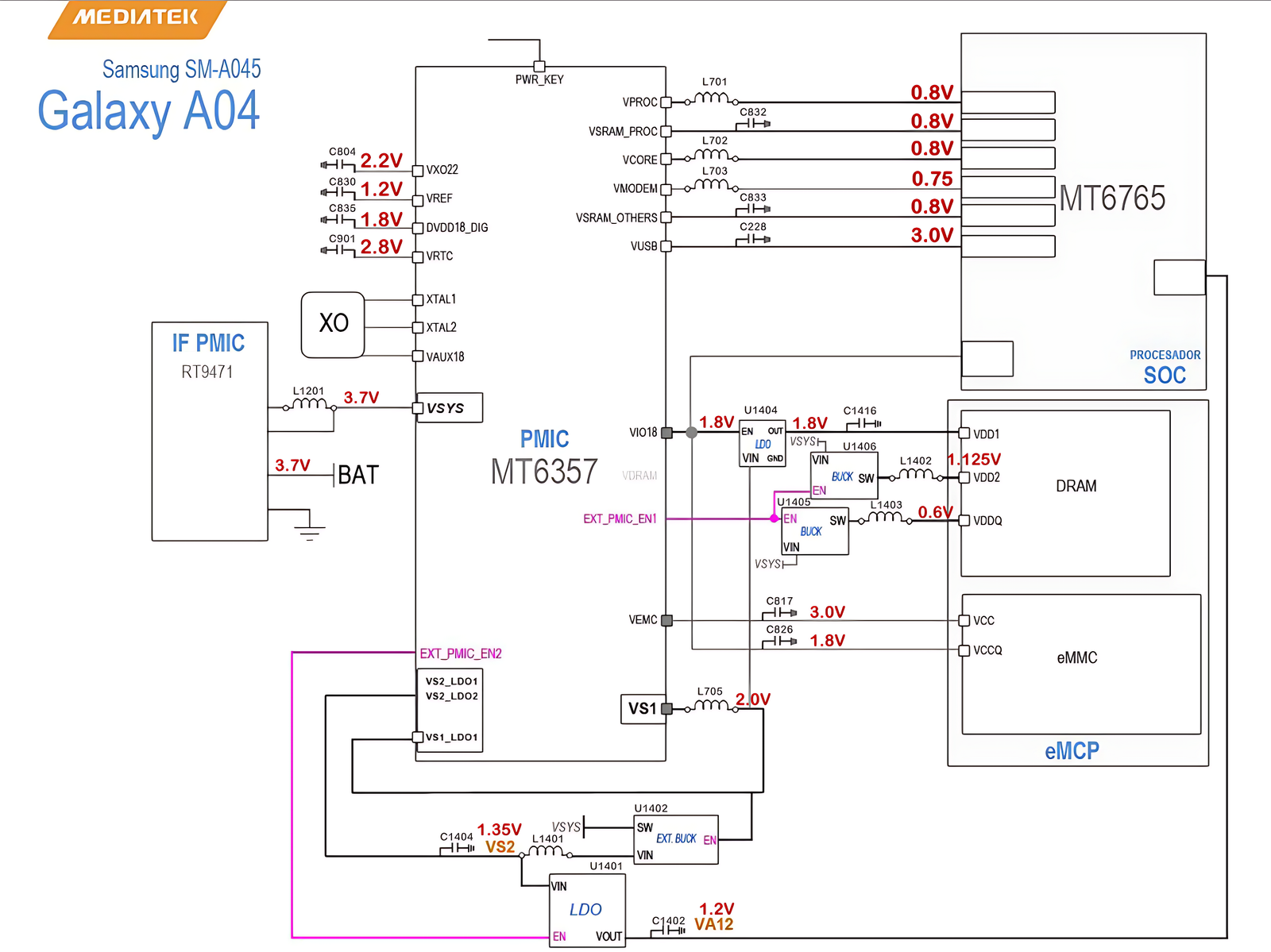
Key Voltage Rails and Their Purpose
- 0.6V →
VDDQ: DRAM I/O voltage - 0.75V →
VMODEM: Modem processor core - 0.8V →
VSRAM_PROC,VSRAM_OTHERS: SRAM domains of the SoC - 0.8V →
VPROC: Main application processor core (CPU) - 1.125V →
VDD1, VDD2: DRAM Core voltage - 1.2V →
VA12: General Analog voltage supply (possibly Audio, Codec, etc.) - 1.35V →
VS2: May power RF components or other analog domains - 1.8V →
VIO18, VEMC: IO interfaces (eMMC, GPIO, PMIC communication) - 2.0V →
VS1: Additional analog or RF domain - 2.2V →
VXO22: Likely for the crystal oscillator - 2.8V →
VRTC: Real-time clock or always-on domain - 3.0V →
VUSB, VCC: USB power and eMMC power
🔍 Detailed Component-wise Power Supply
1. MT6765 SoC (Processor)
VPROC (0.8V)powers the main CPU cores.VSRAM_PROC (0.8V)powers the SRAM in the processor.VMODEM (0.75V)is dedicated to modem functionality.VSRAM_OTHERS (0.8V)is for other SRAM/logic blocks.VDDQ (0.6V)is for DRAM IO interfaces.
2. DRAM
VDD1 / VDD2 (1.125V)for DRAM core supply.VDDQ (0.6V)for data line termination (IO buffers).
3. eMMC (Storage)
VCC (3.0V): NAND Flash core supply.VCCQ (1.8V): IO power supply for eMMC.
4. USB & Peripherals
VUSB (3.0V)powers the USB transceivers.VA12 (1.2V): May support various analog/RF circuits.
5. Always-On & Real-Time Clock
VRTC (2.8V): Keeps the clock and possibly power-on logic alive during standby.
🧠 PMIC MT6357 Working Principle
The PMIC (MT6357) uses internal regulators: Buck converters (for high current), LDOs (for low current, noise-sensitive), and switches. It receives the battery voltage (3.7V) as input and then distributes regulated voltage rails using:
- BUCK converters: Efficient switching regulators for CPU, DRAM, etc.
- LDOs: Low-dropout regulators for clean analog/RF power.
- Power switches: Control ON/OFF of power rails to peripherals.
For example, U1405 and U1406 are Buck regulators managing 0.6V and 1.125V respectively, triggered by EXT_PMIC_EN1.
🔄 Enable Signals
Various power domains are activated using EXT_PMIC_EN1 and EXT_PMIC_EN2 signals from the SoC, controlling the sequencing of power-up.
🧪 Voltage Monitoring
Test points or capacitors (like C832, C804, etc.) allow engineers to monitor voltage stability, ripples, or noise during board-level testing.
⚙️ Why These Voltages?
Every chip (CPU, DRAM, eMMC) requires a specific voltage range to operate reliably. Too high and it damages the component; too low and it causes instability. These values are optimized for power efficiency, thermal management, and performance.
🔚 Conclusion
The MT6357 is a highly integrated PMIC tailored for the MT6765 SoC. It ensures that all voltage domains receive the correct power-on sequence, appropriate voltage levels, and thermal efficiency. Understanding the schematic not only helps in troubleshooting but also provides deep insights into mobile hardware design.
Note: This analysis is based on the official schematic of the Galaxy A04. For hardware debugging or repair, always use an oscilloscope/multimeter to verify actual signals.